8-Layer HDI RF PCB RO4350B 1.6mm ENEPIG Finish Impedance Controlled
(Custom PCBs are tailored products; the images and specifications provided are for reference only.)
Introduction to RO4350B Core and RO4450F Bondply
Rogers RO4350B materials are proprietary woven glass reinforced hydrocarbon/ceramics that provide electrical performance similar to PTFE/woven glass while maintaining manufacturability like epoxy/glass. RO4350B laminates offer tight control on dielectric constant (Dk) and low loss, making them cost-effective alternatives to conventional microwave laminates. They are rated UL 94 V-0 for active devices and high-power RF designs.
The RO4450F bondply is compatible with multi-layer constructions and offers a high post-cure Tg, making it ideal for sequential laminations. It demonstrates improved lateral flow capability, making it suitable for designs with challenging fill requirements.
RO4350B Material Features
Dielectric Constant: DK 3.48 ± 0.05 at 10GHz/23°C
Dissipation Factor: 0.0037 at 10GHz/23°C
Thermal Conductivity: 0.69 W/m/°K
CTE (Coefficient of Thermal Expansion): X-axis 10 ppm/°C, Y-axis 12 ppm/°C, Z-axis 32 ppm/°C
High Tg Value: >280°C
Low Water Absorption: 0.06%
RO4450F Bondply Features
Optimal dielectric constant (Dk 3.52±0.05)
Low dissipation factor (Df 0.004 @10GHz)
Excellent thermal conductivity (0.65 W/m/K)
Superior lamination compatibility
Multiple lamination cycle capability
PCB Construction Details
Base Material: RO4350B
Layer Count: 8-layer
Board Dimensions: 96.4 mm x 163.9 mm (3 Types = 3 PCS, +/- 0.15 mm)
Minimum Trace/Space: 4/6 mils
Minimum Hole Size: 0.4 mm
Blind Vias: GTL-L7, L3-GBL, GTL-L2, L7-GBL, GTL-L3, GTL-L4, GTL-L5, L5-GBL, L4-GBL, GTL-L6, L6-GBL, L2-GBL, mechanical drill.
Finished Board Thickness: 1.8 mm
Finished Copper Weight: 1 oz (1.4 mils) outer layers; 1 oz (1.4 mils) / 0.5 oz (0.7 mils) inner layers
Via Plating Thickness: 20 µm
Surface Finish: Electroless Nickel Immersion Gold
Top Silkscreen: White
Bottom Silkscreen: White
Top Solder Mask: Green
Bottom Solder Mask: Green
Vias: All are resin filled and capped
Testing: 100% Electrical test prior to shipment
Impedance Control: 50 ohm on various layers
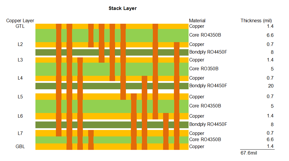
PCB Stackup: 8-layer Rigid PCB
Copper Layer 1: 17 µm + plating
RO4350B Core: 0.168 mm (6.6 mils)
Copper Layer 2: 17 µm
8 mil RO4450F Bondply
Copper Layer 3: 35 µm
RO4350B Core: 0.127 mm (5 mils)
Copper Layer 4: 17 µm
20 mil RO4450F Bondply
Copper Layer 5: 17 µm
RO4350B Core: 0.127 mm (5 mils)
Copper Layer 6: 35 µm
8 mil RO4450F Bondply
Copper Layer 7: 17 µm
RO4350B Core: 0.168 mm (6.6 mils)
Copper Layer 8: 17 µm + plating
PCB Statistics
Components: 76
Total Pads: 303
Thru Hole Pads: 117
Top SMT Pads: 121
Bottom SMT Pads: 65
Vias: 335
Nets: 6
Typical Applications
Cellular Base Station Antennas
RF Identification Tags
Automotive Radar and Sensors
LNBs for Direct Broadcast Satellites
Artwork and Quality Standards
The artwork supplied for this PCB is in the Gerber RS-274-X format, adhering to IPC-Class-2 quality standards. This product is available for distribution worldwide.
